


XILINX Zynq-7000 SoC PCie FMC HPC FPGA Development Board XC7Z100
- Call for Pricing
Description of product
Product Parameters
Main Parameters
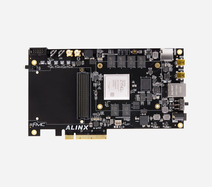
FPGA Board AX7450
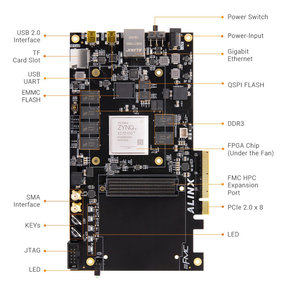
FPGA Chip XC7Z100-2FFG900
Kernel Dual-Core ARM Cortex-A9, Main Frequency 800MHz
PS-end RAM 1GB DDR3, Data Rate 1066Mbps, 32bit
PL-end RAM 2GB DDR3, Data Rate1600Mbps, 64bit
Transceivers 16 -Channels Support PCIE Gen2 x8
Speed Grades -2
Working Temperature -40°C~85°C
Look Up Tables (LUTs) 277,400
CLB Flip-Flops 554,800
EMMC FLASH 8GB
Chip Level Industrial Grade
Logic Cells 444k
Multiplier 2020 ( 18x 25MACCs )
Block RAM 26.5Mbit
QSPI FLASH 512Mbit
Interface and Function
DDR3 2x 512MB DDR3, a total of 1GB, 32bit Bus
4x 512MB DDR3, a total of 2GB, 64bit bus
QSPI Flash 2x 256Mbit, Used as FPGA User Data Storage
EMMC Flash 8GB EMMC FLASH Memory Chip is Mounted on the PS Side Used as User Stores Operating System Files or other User Data
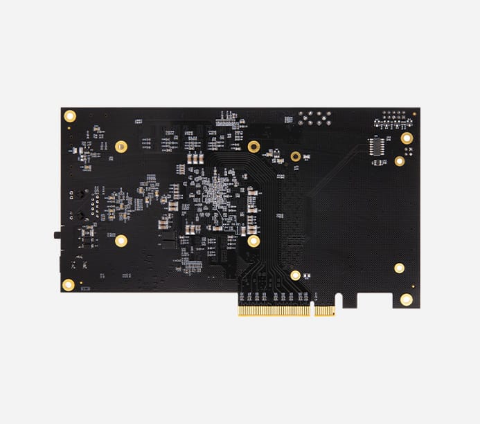
PCIe 2.0 x 8 Support PCI Express 2.0 Standard, Standard PCIe x8 High-Speed Data Transmission Interface. Each rate can be up to 5GBaud
Ethernet Interface Gigabit Ethernet RJ-45 Interfaces for Ethernet Data Exchange
JTAG JTAG Interface to Debug and Download ZYNQ System
USB 2.0 Used for OTG Communication with PC or USB Device
USB Uart Used for Serial Communication with PC or External Devices
TF Card Slot SD Card for Store Operating System Image and File System
Crystal Oscillator 33.333Mhz Provide Stable Clock Source for the PS System
50MHz, Provide Extra Clock for PL Logic
Programmable Clock Chip provide the Clock Source for GTX and a Reference Clock for PCIE, SFP and DDR operations
SMA Interface 2 SMA Interfaces, Connect External Trigger Signal or Clock Signal
LED1 Power Indicator LED, 1 DONE Indicator LED, 4 User Debugging LED, 1 Front Panel Dual-color LED.
KEYs 2 Keys, 1 Reset Key, 1 PL User Key.
Power Supply Parameters
Voltage Input +12V DC
Current Input Max. Current 3A
Package List
FPGA Board 1
DC Fan 1
USB Downloader Cable 1 Set
TF Card 1
12V Power Adapter 1
Card Reader 1
Mini USB Cable 2
Structure Size
Size Dimension
7.49 inch x 4.20 inch
Number of Layers
4-Layer PCB


