
-
TRANSDUCERS
- TRANSDUCERS
-
BASIC COMPONENTS DK
- BASIC COMPONENTS DK
-
MARKETPLACE
- MARKETPLACE
-
DEVELOPMENT BOARDS & KITS
- DEVELOPMENT BOARDS & KITS
-
CABLE ASSEMBLIES
- CABLE ASSEMBLIES
-
RF AND WIRELESS
- RF AND WIRELESS
-
BOXES ENCLOSURES RACKS
- BOXES ENCLOSURES RACKS
-
AUDIO PRODUCTS
- AUDIO PRODUCTS
-
ARTILA
- ARTILA
-
FANS-BLOWERS-THERMAL MANAGEMENT
- FANS-BLOWERS-THERMAL MANAGEMENT
-
WIRELESS MODULES
- WIRELESS MODULES
-
TERMINALS
- TERMINALS
-
Cables/Wires
- Cables/Wires
-
SINGLE BOARD COMPUTER
- SINGLE BOARD COMPUTER
-
BREAKOUT BOARDS
- BREAKOUT BOARDS
-
LED
- LED
-
TEST AND MEASUREMENT
- TEST AND MEASUREMENT
-
POTENTIONMETERS AND VARIABLE RESISTORS
- POTENTIONMETERS AND VARIABLE RESISTORS
-
DEVELOPMENT BOARDS AND IC's
- DEVELOPMENT BOARDS AND IC's
-
EMBEDDED COMPUTERS
- EMBEDDED COMPUTERS
-
OPTOELECTRONICS
- OPTOELECTRONICS
-
INDUSTRAL AUTOMATION AND CONTROL
- INDUSTRAL AUTOMATION AND CONTROL
-
COMPUTER EQUIPMENT
- COMPUTER EQUIPMENT
-
CONNECTORS & INTERCONNECTS
- CONNECTORS & INTERCONNECTS
-
MAKER/DIY EDUCATIONAL
- MAKER/DIY EDUCATIONAL
-
TOOLS
- TOOLS
-
MOTORS/ACTUATORS/SOLEENOIDS/DRIVERS
- MOTORS/ACTUATORS/SOLEENOIDS/DRIVERS
-
FPGA HARDWARE
- FPGA HARDWARE
-
POWER SUPPLIES
- POWER SUPPLIES
-
ROBOTICS & AUTOMATION
- ROBOTICS & AUTOMATION

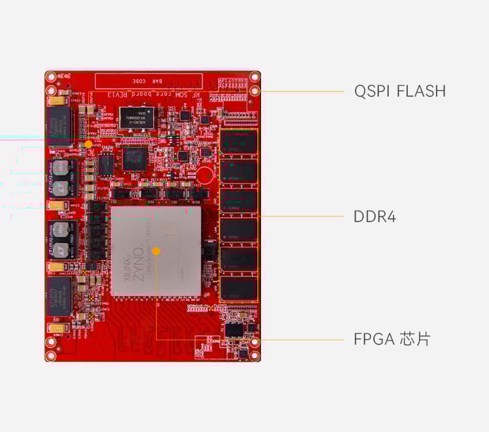
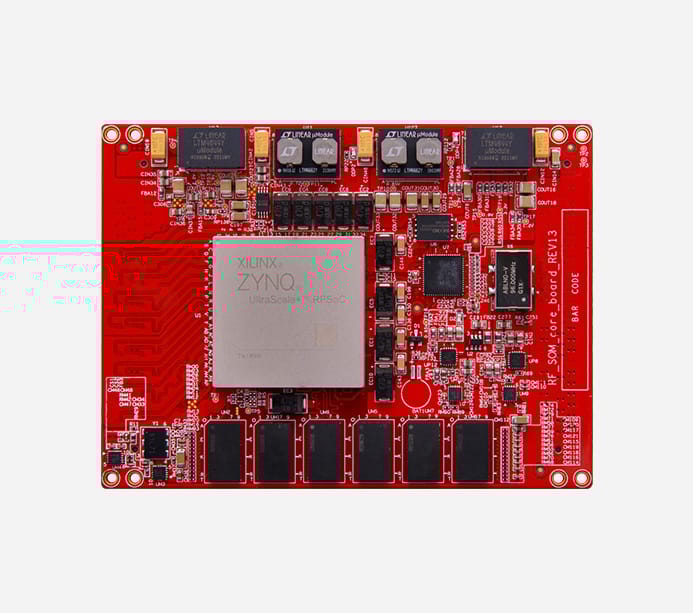
RFSOM integrates hardware and software to help you provide a prototype of a high-performance wireless receiver system and perform air signal acquisition and analysis. In addition, RFSOM adopts a RF direct sampling structure with eight independent transmitter and receiver channels. It integrates a programmable Xilinx RFSoC FPGA minimum system, supports software defined radio development architecture, has large bandwidth and large-scale computing processing capabilities, and can be used for wireless communication prototype verification, spectrum monitoring, signal intelligence, and broadband acquisition and recording applications. The RFSOM is also equipped with a 19.2 MHz constant temperature crystal oscillator (OCXO) reference clock, which improves frequency accuracy and synchronization.
The main interfaces and resources of FPGA
Core configuration:
· Intgrateed Device of ZU47DR RF System on Chip (RFSoC)
· Equipped with built-in digital up and down conversion and interpolation extraction functions
· Supports 8-way transmission and 8-way reception
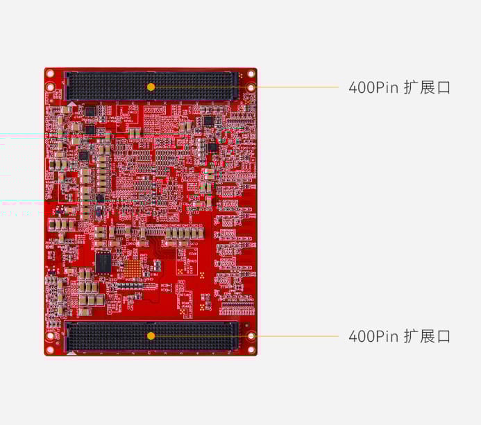
SOM minimum system:
Simulate RFMC connectors
1. ADC/DAC fully differential lead out, supporting DC or AC coupling
2. VCM export supports setting common mode level
Digital RFMC connector
1. GTY export, supporting PCIE4.0X8 rate transmission
2. MIO export, supporting expansion of Ethernet, USB and other peripheral interfaces, supporting peripheral level
3. GTR export, supporting expansion of storage interfaces such as Sata/PCIE hard drives, and supporting external device levels
4. HD IO output, supporting peripheral device level
CACHE
1. PL DDR4 32bit single channel DDR4 cache supports 2600MHz, 2GB capacity
2. PS DDR4 64bit single channel DDR4 cache supports 2133MHz and 4GB capacity
3. QSPI flash, 1GB capacity
Debug Interface
1. JTAG lead out
2. Reset signal lead out
Cascading interface:
·Built in LMK04828 dedicated clock circuit
·Integrated 19.2MHz OCXO
·External clock synchronization
·Trigger synchronization
·SYSREF synchronization
Power supply:
·5V single power supply
·Heat sink embedded fan
·Typical power consumption, running 50% logic,8TX&8RX,TBD Watt
Sampling rate support:
·API supports real-time bandwidth of 30.72/61.44/122.88/245.76/491.52/983.04MHz (maximum support for 2.5GHz bandwidth)
Product parameters
Core board -ACRF47
FPGA model -XCZU47DR-2FFVE1156I
kernel CPU -Quad-core ARM Cortex-A53, MPCore/Dual-core ARM Cortex-R5F, MPCore
Memory -PS DDR4,4GB /PL DDR4,2GB
14 bit 5.0GSPS RF-ADC -8
14 bit 9.85GSPS RF-DAC -8
Decimation/ interpolation -1x, 2x, 3x, 4x, 5x, 6x, 8x, 10x, 12x, 16x, 20x, 24x, 40x
GTY / GTR -PL GTY8 / PS GTR4
System Logic Cell -930K
CLB LUTs -425K
Max.Dist.RAM -13.0Mb
Total Block RAM -38.0Mb
UltraRAM -22.5Mb
DSP Slices -4272
PCIe Gen4 x8 -1
Applications
-
5G FR1/FR2 RF and baseband
-
Phased array system
-
Radar system
-
Software Radio
-
Spectrum monitoring
-
Medical system
- Home
- ALINX Xilinx FPGA
- Xilinx Zynq UltraScale+RFSoC Gen3 ZU47DR FPGA chip integrated RF direct sampling data converter high-speed transceiver ZU47DR


Xilinx Zynq UltraScale+RFSoC Gen3 ZU47DR FPGA chip integrated RF direct sampling data converter high-speed transceiver ZU47DR
SIZE GUIDE
Your enquiry has been sent
Product Enquiry Form
Leave us a message for futher information.
- Lead time is 3-4 weeks
Description of product
RFSOM integrates hardware and software to help you provide a prototype of a high-performance wireless receiver system and perform air signal acquisition and analysis. In addition, RFSOM adopts a RF direct sampling structure with eight independent transmitter and receiver channels. It integrates a programmable Xilinx RFSoC FPGA minimum system, supports software defined radio development architecture, has large bandwidth and large-scale computing processing capabilities, and can be used for wireless communication prototype verification, spectrum monitoring, signal intelligence, and broadband acquisition and recording applications. The RFSOM is also equipped with a 19.2 MHz constant temperature crystal oscillator (OCXO) reference clock, which improves frequency accuracy and synchronization.
The main interfaces and resources of FPGA
Core configuration:
· Intgrateed Device of ZU47DR RF System on Chip (RFSoC)
· Equipped with built-in digital up and down conversion and interpolation extraction functions
· Supports 8-way transmission and 8-way reception
SOM minimum system:
Simulate RFMC connectors
1. ADC/DAC fully differential lead out, supporting DC or AC coupling
2. VCM export supports setting common mode level
Digital RFMC connector
1. GTY export, supporting PCIE4.0X8 rate transmission
2. MIO export, supporting expansion of Ethernet, USB and other peripheral interfaces, supporting peripheral level
3. GTR export, supporting expansion of storage interfaces such as Sata/PCIE hard drives, and supporting external device levels
4. HD IO output, supporting peripheral device level
CACHE
1. PL DDR4 32bit single channel DDR4 cache supports 2600MHz, 2GB capacity
2. PS DDR4 64bit single channel DDR4 cache supports 2133MHz and 4GB capacity
3. QSPI flash, 1GB capacity
Debug Interface
1. JTAG lead out
2. Reset signal lead out
Cascading interface:
·Built in LMK04828 dedicated clock circuit
·Integrated 19.2MHz OCXO
·External clock synchronization
·Trigger synchronization
·SYSREF synchronization
Power supply:
·5V single power supply
·Heat sink embedded fan
·Typical power consumption, running 50% logic,8TX&8RX,TBD Watt
Sampling rate support:
·API supports real-time bandwidth of 30.72/61.44/122.88/245.76/491.52/983.04MHz (maximum support for 2.5GHz bandwidth)
Product parameters
Core board -ACRF47
FPGA model -XCZU47DR-2FFVE1156I
kernel CPU -Quad-core ARM Cortex-A53, MPCore/Dual-core ARM Cortex-R5F, MPCore
Memory -PS DDR4,4GB /PL DDR4,2GB
14 bit 5.0GSPS RF-ADC -8
14 bit 9.85GSPS RF-DAC -8
Decimation/ interpolation -1x, 2x, 3x, 4x, 5x, 6x, 8x, 10x, 12x, 16x, 20x, 24x, 40x
GTY / GTR -PL GTY8 / PS GTR4
System Logic Cell -930K
CLB LUTs -425K
Max.Dist.RAM -13.0Mb
Total Block RAM -38.0Mb
UltraRAM -22.5Mb
DSP Slices -4272
PCIe Gen4 x8 -1
Applications
-
5G FR1/FR2 RF and baseband
-
Phased array system
-
Radar system
-
Software Radio
-
Spectrum monitoring
-
Medical system
Related products


NEWSLETTER
Subscribe to get Email Updates!
Thanks for subscribe.
Your response has been recorded.
INFORMATION
ACCOUNT
ADDRESS
Tenet Technetronics# 2514/U, 7th 'A' Main Road, Opp. to BBMP Swimming Pool, Hampinagar, Vijayanagar 2nd Stage.
Bangalore
Karnataka - 560104
IN
Tenet Technetronics focuses on “Simplifying Technology for Life” and has been striving to deliver the same from the day of its inception since 2007. Founded by young set of graduates with guidance from ardent professionals and academicians the company focuses on delivering high quality products to its customers at the right cost considering the support and lifelong engagement with customers. “We don’t believe in a sell and forget model “and concentrate and building relationships with customers that accelerates, enhances as well as provides excellence in their next exciting project.