- TRANSDUCERS
- TRANSDUCERS
- BASIC COMPONENTS DK
- BASIC COMPONENTS DK
- MARKETPLACE
- MARKETPLACE
- DEVELOPMENT BOARDS & KITS
- DEVELOPMENT BOARDS & KITS
- CABLE ASSEMBLIES
- CABLE ASSEMBLIES
- RF AND WIRELESS
- RF AND WIRELESS
- BOXES ENCLOSURES RACKS
- BOXES ENCLOSURES RACKS
- AUDIO PRODUCTS
- AUDIO PRODUCTS
- FANS-BLOWERS-THERMAL MANAGEMENT
- FANS-BLOWERS-THERMAL MANAGEMENT
- WIRELESS MODULES
- WIRELESS MODULES
- TERMINALS
- TERMINALS
- Cables/Wires
- Cables/Wires
- SINGLE BOARD COMPUTER
- SINGLE BOARD COMPUTER
- BREAKOUT BOARDS
- BREAKOUT BOARDS
- LED
- LED
- TEST AND MEASUREMENT
- TEST AND MEASUREMENT
- POTENTIONMETERS AND VARIABLE RESISTORS
- POTENTIONMETERS AND VARIABLE RESISTORS
- DEVELOPMENT BOARDS AND IC's
- DEVELOPMENT BOARDS AND IC's
- EMBEDDED COMPUTERS
- EMBEDDED COMPUTERS
- OPTOELECTRONICS
- OPTOELECTRONICS
- INDUSTRAL AUTOMATION AND CONTROL
- INDUSTRAL AUTOMATION AND CONTROL
- COMPUTER EQUIPMENT
- COMPUTER EQUIPMENT
- CONNECTORS & INTERCONNECTS
- CONNECTORS & INTERCONNECTS
- MAKER/DIY EDUCATIONAL
- MAKER/DIY EDUCATIONAL
- TOOLS
- TOOLS
- MOTORS/ACTUATORS/SOLEENOIDS/DRIVERS
- MOTORS/ACTUATORS/SOLEENOIDS/DRIVERS
- FPGA HARDWARE
- FPGA HARDWARE
- ROBOTICS & AUTOMATION
- ROBOTICS & AUTOMATION
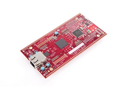
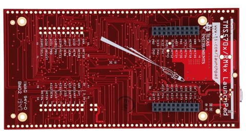
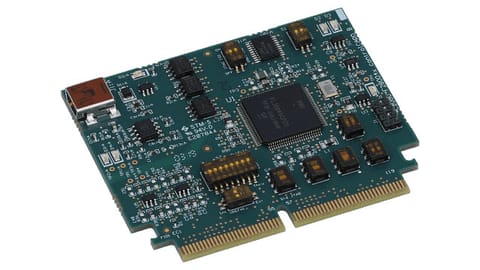
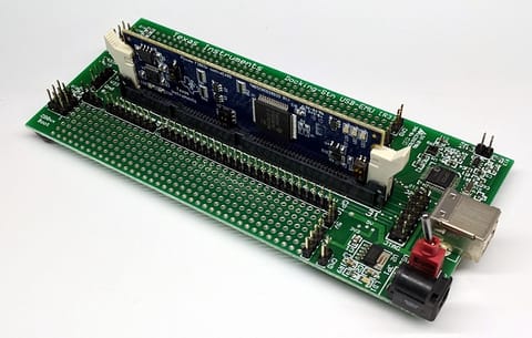
C2000™ 32-bit microcontrollers are optimized for processing, sensing, and actuation to improve closed-loop performance in real-time control applications such as industrial motor drives; solar inverters and digital power; electrical vehicles and transportation; motor control; and sensing and signal processing. The C2000 line includes the Delfino™ Premium Performance family and the Piccolo™ Entry Performance family.
TMS320C2000™ 32-bit microcontrollers are optimized for processing, sensing, and actuation to improve closed-loop performance in real-time control applications. The C2000™ microcontrollers line includes the Delfino™ Premium Performance microcontroller family and the Piccolo™ Entry Performance microcontroller family.
The TMS320F28335, TMS320F28334, TMS320F28333, TMS320F28332, TMS320F28235, TMS320F28234, and TMS320F28232 devices, members of the TMS320C28x/Delfino™ DSC/MCU generation, are highly integrated, high-performance solutions for demanding control applications.
Throughout this document, the devices are abbreviated as F28335, F28334, F28333, F28332, F28235, F28234, and F28232, respectively. F2833x Device Comparison and F2823x Device Comparison provide a summary of features for each device.
Features
- High-performance static CMOS technology
- Up to 150 MHz (6.67-ns cycle time)
- 1.9-V/1.8-V core, 3.3-V I/O design
- High-performance 32-bit CPU (TMS320C28x)
- IEEE 754 single-precision Floating-Point Unit (FPU) (F2833x only)
- 16 × 16 and 32 × 32 MAC operations
- 16 × 16 dual MAC
- Harvard bus architecture
- Fast interrupt response and processing
- Unified memory programming model
- Code-efficient (in C/C++ and Assembly)
- Six-channel DMA controller (for ADC, McBSP, ePWM, XINTF, and SARAM)
- 16-bit or 32-bit External Interface (XINTF)
- More than 2M × 16 address reach
- On-chip memory
- F28335, F28333, F28235:
256K × 16 flash, 34K × 16 SARAM - F28334, F28234:
128K × 16 flash, 34K × 16 SARAM - F28332, F28232:
64K × 16 flash, 26K × 16 SARAM - 1K × 16 OTP ROM
- F28335, F28333, F28235:
- Boot ROM (8K × 16)
- With software boot modes (through SCI, SPI, CAN, I2C, McBSP, XINTF, and parallel I/O)
- Standard math tables
- Clock and system control
- On-chip oscillator
- Watchdog timer module
- GPIO0 to GPIO63 pins can be connected to one of the eight external core interrupts
- Peripheral Interrupt Expansion (PIE) block that supports all 58 peripheral interrupts
- 128-bit security key/lock
- Protects flash/OTP/RAM blocks
- Prevents firmware reverse-engineering
- Enhanced control peripherals
- Up to 18 PWM outputs
- Up to 6 HRPWM outputs with 150-ps MEP resolution
- Up to 6 event capture inputs
- Up to 2 Quadrature Encoder interfaces
- Up to 8 32-bit timers
(6 for eCAPs and 2 for eQEPs) - Up to 9 16-bit timers
(6 for ePWMs and 3 XINTCTRs)
- Three 32-bit CPU timers
- Serial port peripherals
- Up to 2 CAN modules
- Up to 3 SCI (UART) modules
- Up to 2 McBSP modules (configurable as SPI)
- One SPI module
- One Inter-Integrated Circuit (I2C) bus
- 12-bit ADC, 16 channels
- 80-ns conversion rate
- 2 × 8 channel input multiplexer
- Two sample-and-hold
- Single/simultaneous conversions
- Internal or external reference
- Up to 88 individually programmable, multiplexed GPIO pins with input filtering
- JTAG boundary scan support
- IEEE Standard 1149.1-1990 Standard Test Access Port and Boundary Scan Architecture
- Advanced emulation features
- Analysis and breakpoint functions
- Real-time debug using hardware
- Development support includes
- ANSI C/C++ compiler/assembler/linker
- Code Composer Studio™ IDE
- DSP/BIOS™ and SYS/BIOS
- Digital motor control and digital power software libraries
- Low-power modes and power savings
- IDLE, STANDBY, HALT modes supported
- Disable individual peripheral clocks
- Endianness: Little endian
- Package options:
- Lead-free, green packaging
- 176-ball plastic Ball Grid Array (BGA) (ZJZ)
- 179-ball MicroStar BGA™ (ZHH)
- 176-pin Low-Profile Quad Flatpack (LQFP) (PGF)
- 176-pin Thermally Enhanced Low-Profile Quad Flatpack (HLQFP) (PTP)
- Temperature options:
- A: –40°C to 85°C (PGF, ZHH, ZJZ)
- S: –40°C to 125°C (PTP, ZJZ)
- Q: –40°C to 125°C (PTP, ZJZ)
(AEC Q100 qualification for automotive applications)
- Home
- DEVELOPMENT BOARDS AND IC's
- Texas Instruments
- TMS320F28335
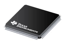
TMS320F28335
SIZE GUIDE
- Shipping in 10-12 Working days
Description of product
C2000™ 32-bit microcontrollers are optimized for processing, sensing, and actuation to improve closed-loop performance in real-time control applications such as industrial motor drives; solar inverters and digital power; electrical vehicles and transportation; motor control; and sensing and signal processing. The C2000 line includes the Delfino™ Premium Performance family and the Piccolo™ Entry Performance family.
TMS320C2000™ 32-bit microcontrollers are optimized for processing, sensing, and actuation to improve closed-loop performance in real-time control applications. The C2000™ microcontrollers line includes the Delfino™ Premium Performance microcontroller family and the Piccolo™ Entry Performance microcontroller family.
The TMS320F28335, TMS320F28334, TMS320F28333, TMS320F28332, TMS320F28235, TMS320F28234, and TMS320F28232 devices, members of the TMS320C28x/Delfino™ DSC/MCU generation, are highly integrated, high-performance solutions for demanding control applications.
Throughout this document, the devices are abbreviated as F28335, F28334, F28333, F28332, F28235, F28234, and F28232, respectively. F2833x Device Comparison and F2823x Device Comparison provide a summary of features for each device.
Features
- High-performance static CMOS technology
- Up to 150 MHz (6.67-ns cycle time)
- 1.9-V/1.8-V core, 3.3-V I/O design
- High-performance 32-bit CPU (TMS320C28x)
- IEEE 754 single-precision Floating-Point Unit (FPU) (F2833x only)
- 16 × 16 and 32 × 32 MAC operations
- 16 × 16 dual MAC
- Harvard bus architecture
- Fast interrupt response and processing
- Unified memory programming model
- Code-efficient (in C/C++ and Assembly)
- Six-channel DMA controller (for ADC, McBSP, ePWM, XINTF, and SARAM)
- 16-bit or 32-bit External Interface (XINTF)
- More than 2M × 16 address reach
- On-chip memory
- F28335, F28333, F28235:
256K × 16 flash, 34K × 16 SARAM - F28334, F28234:
128K × 16 flash, 34K × 16 SARAM - F28332, F28232:
64K × 16 flash, 26K × 16 SARAM - 1K × 16 OTP ROM
- F28335, F28333, F28235:
- Boot ROM (8K × 16)
- With software boot modes (through SCI, SPI, CAN, I2C, McBSP, XINTF, and parallel I/O)
- Standard math tables
- Clock and system control
- On-chip oscillator
- Watchdog timer module
- GPIO0 to GPIO63 pins can be connected to one of the eight external core interrupts
- Peripheral Interrupt Expansion (PIE) block that supports all 58 peripheral interrupts
- 128-bit security key/lock
- Protects flash/OTP/RAM blocks
- Prevents firmware reverse-engineering
- Enhanced control peripherals
- Up to 18 PWM outputs
- Up to 6 HRPWM outputs with 150-ps MEP resolution
- Up to 6 event capture inputs
- Up to 2 Quadrature Encoder interfaces
- Up to 8 32-bit timers
(6 for eCAPs and 2 for eQEPs) - Up to 9 16-bit timers
(6 for ePWMs and 3 XINTCTRs)
- Three 32-bit CPU timers
- Serial port peripherals
- Up to 2 CAN modules
- Up to 3 SCI (UART) modules
- Up to 2 McBSP modules (configurable as SPI)
- One SPI module
- One Inter-Integrated Circuit (I2C) bus
- 12-bit ADC, 16 channels
- 80-ns conversion rate
- 2 × 8 channel input multiplexer
- Two sample-and-hold
- Single/simultaneous conversions
- Internal or external reference
- Up to 88 individually programmable, multiplexed GPIO pins with input filtering
- JTAG boundary scan support
- IEEE Standard 1149.1-1990 Standard Test Access Port and Boundary Scan Architecture
- Advanced emulation features
- Analysis and breakpoint functions
- Real-time debug using hardware
- Development support includes
- ANSI C/C++ compiler/assembler/linker
- Code Composer Studio™ IDE
- DSP/BIOS™ and SYS/BIOS
- Digital motor control and digital power software libraries
- Low-power modes and power savings
- IDLE, STANDBY, HALT modes supported
- Disable individual peripheral clocks
- Endianness: Little endian
- Package options:
- Lead-free, green packaging
- 176-ball plastic Ball Grid Array (BGA) (ZJZ)
- 179-ball MicroStar BGA™ (ZHH)
- 176-pin Low-Profile Quad Flatpack (LQFP) (PGF)
- 176-pin Thermally Enhanced Low-Profile Quad Flatpack (HLQFP) (PTP)
- Temperature options:
- A: –40°C to 85°C (PGF, ZHH, ZJZ)
- S: –40°C to 125°C (PTP, ZJZ)
- Q: –40°C to 125°C (PTP, ZJZ)
(AEC Q100 qualification for automotive applications)
NEWSLETTER
Subscribe to get Email Updates!
Thanks for subscribe.
Your response has been recorded.
INFORMATION
ACCOUNT
ADDRESS
Tenet Technetronics# 2514/U, 7th 'A' Main Road, Opp. to BBMP Swimming Pool, Hampinagar, Vijayanagar 2nd Stage.
Bangalore
Karnataka - 560104
IN
Tenet Technetronics focuses on “Simplifying Technology for Life” and has been striving to deliver the same from the day of its inception since 2007. Founded by young set of graduates with guidance from ardent professionals and academicians the company focuses on delivering high quality products to its customers at the right cost considering the support and lifelong engagement with customers. “We don’t believe in a sell and forget model “and concentrate and building relationships with customers that accelerates, enhances as well as provides excellence in their next exciting project.


