- TRANSDUCERS
- TRANSDUCERS
- BASIC COMPONENTS DK
- BASIC COMPONENTS DK
- MARKETPLACE
- MARKETPLACE
- DEVELOPMENT BOARDS & KITS
- DEVELOPMENT BOARDS & KITS
- CABLE ASSEMBLIES
- CABLE ASSEMBLIES
- RF AND WIRELESS
- RF AND WIRELESS
- BOXES ENCLOSURES RACKS
- BOXES ENCLOSURES RACKS
- AUDIO PRODUCTS
- AUDIO PRODUCTS
- FANS-BLOWERS-THERMAL MANAGEMENT
- FANS-BLOWERS-THERMAL MANAGEMENT
- WIRELESS MODULES
- WIRELESS MODULES
- TERMINALS
- TERMINALS
- Cables/Wires
- Cables/Wires
- SINGLE BOARD COMPUTER
- SINGLE BOARD COMPUTER
- BREAKOUT BOARDS
- BREAKOUT BOARDS
- LED
- LED
- TEST AND MEASUREMENT
- TEST AND MEASUREMENT
- POTENTIONMETERS AND VARIABLE RESISTORS
- POTENTIONMETERS AND VARIABLE RESISTORS
- DEVELOPMENT BOARDS AND IC's
- DEVELOPMENT BOARDS AND IC's
- EMBEDDED COMPUTERS
- EMBEDDED COMPUTERS
- OPTOELECTRONICS
- OPTOELECTRONICS
- INDUSTRAL AUTOMATION AND CONTROL
- INDUSTRAL AUTOMATION AND CONTROL
- COMPUTER EQUIPMENT
- COMPUTER EQUIPMENT
- CONNECTORS & INTERCONNECTS
- CONNECTORS & INTERCONNECTS
- MAKER/DIY EDUCATIONAL
- MAKER/DIY EDUCATIONAL
- TOOLS
- TOOLS
- MOTORS/ACTUATORS/SOLEENOIDS/DRIVERS
- MOTORS/ACTUATORS/SOLEENOIDS/DRIVERS
- FPGA HARDWARE
- FPGA HARDWARE
- ROBOTICS & AUTOMATION
- ROBOTICS & AUTOMATION
The Stratix® V GX FPGA Development Kit provides a complete design environment that includes all the hardware and software you need to begin developing FPGA designs immediately. You can use this development kit to do the following:
- Develop and test PCI Express® (PCIe®) designs at data rates up to Gen3 using the PCIe short card form factor-compliant development board
- Develop and test memory subsystems for DDR3, QDR II+, or RLDRAM II memories
- Use the high-speed mezzanine card (HSMC) connectors to interface to one of over 35 different HSMCs provided by partners, supporting protocols, such as Serial RapidIO®, 10 Gbps Ethernet, SONET, CPRI, OBSAI, and others
Development Kit Contents
The Stratix V GX FPGA Development Kit features the following:
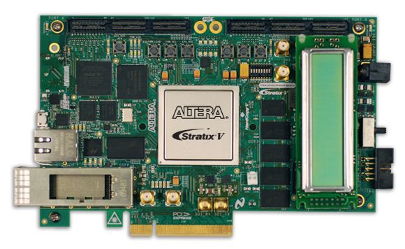
- Stratix V GX FPGA development board (see Figure 1)
- Featured device:
- Stratix V GX FPGA: 5SGXEA7K2F40C2N
- Configuration, status, and setup elements
- JTAG
- On-board USB-BlasterTM II cable
- Fast passive parallel (FPP) configuration via MAX® V device and flash memory
- One reset config push button
- One CPU reset push button
- Two configuration push buttons
- Clocks
- 50 MHz, 125 MHz, 100 MHz, and 148.5 MHz programmable oscillators
- SMA input (LVPECL)
- General user input and output
- 10/100/1000Mbps Ethernet PHY (SGMII) with RJ-45 (copper) connector
- 16x2 character LCD
- One 8-position dual in-line package (DIP) switch
- Sixteen user LEDs
- Three user push buttons
- Memory devices
- DDR3 SDRAM (1,152 MB, x72 bit wide)
- QDR II+ SRAM (4.5 MB, 2 Mb x18 bit wide)
- Footprint compatible to QDR II 4 Mb x18 bit wide
- RLDRAM II (72 MB CIO RLDRAM II with an 18 bit data bus)
- Component and interfaces
- PCIe x8 edge connector
- Two HSMC connectors
- SMB for serial digital interface (SDI) input and output
- QSFP optical cage
- 10/100/1000Mbps Ethernet PHY (SGMII) with RJ-45 (copper) connector
- Power
- Laptop DC input
- PCIe edge connector
- Nios® II processor web server and remote system update
- Loopback and debug HSMC cards
- Power adapter and cables
- Stratix V GX FPGA Development Kit software content
- Complete documentation
- User guide
- Reference manual
- Board schematics and layout design files
- GUI-based Board Test System
- Includes complete Quartus software projects with open source RTL
- Board Update Portal
- Includes complete Quartus software projects with open source RTL
- Quartus Prime design software, Development Kit Edition (DKE)
- License to use full version of Quartus Prime design software for one year
- Complete documentation
- Featured device:
- Home
- FPGA HARDWARE
- INTEL FPGA
- Stratix V GX FPGA Development Kit
Stratix V GX FPGA Development Kit
SIZE GUIDE
- Shipping in 10-12 Working days
- http://cdn.storehippo.com/s/59c9e4669bd3e7c70c5f5e6c/ms.products/5a0ab1ee6d2b85b55830807e/images/5a0ab1ee6d2b85b55830807f/5a0ab15790d0969044b2dd1d/5a0ab15790d0969044b2dd1d.jpg
Description of product
The Stratix® V GX FPGA Development Kit provides a complete design environment that includes all the hardware and software you need to begin developing FPGA designs immediately. You can use this development kit to do the following:
- Develop and test PCI Express® (PCIe®) designs at data rates up to Gen3 using the PCIe short card form factor-compliant development board
- Develop and test memory subsystems for DDR3, QDR II+, or RLDRAM II memories
- Use the high-speed mezzanine card (HSMC) connectors to interface to one of over 35 different HSMCs provided by partners, supporting protocols, such as Serial RapidIO®, 10 Gbps Ethernet, SONET, CPRI, OBSAI, and others
Development Kit Contents
The Stratix V GX FPGA Development Kit features the following:
- Stratix V GX FPGA development board (see Figure 1)
- Featured device:
- Stratix V GX FPGA: 5SGXEA7K2F40C2N
- Configuration, status, and setup elements
- JTAG
- On-board USB-BlasterTM II cable
- Fast passive parallel (FPP) configuration via MAX® V device and flash memory
- One reset config push button
- One CPU reset push button
- Two configuration push buttons
- Clocks
- 50 MHz, 125 MHz, 100 MHz, and 148.5 MHz programmable oscillators
- SMA input (LVPECL)
- General user input and output
- 10/100/1000Mbps Ethernet PHY (SGMII) with RJ-45 (copper) connector
- 16x2 character LCD
- One 8-position dual in-line package (DIP) switch
- Sixteen user LEDs
- Three user push buttons
- Memory devices
- DDR3 SDRAM (1,152 MB, x72 bit wide)
- QDR II+ SRAM (4.5 MB, 2 Mb x18 bit wide)
- Footprint compatible to QDR II 4 Mb x18 bit wide
- RLDRAM II (72 MB CIO RLDRAM II with an 18 bit data bus)
- Component and interfaces
- PCIe x8 edge connector
- Two HSMC connectors
- SMB for serial digital interface (SDI) input and output
- QSFP optical cage
- 10/100/1000Mbps Ethernet PHY (SGMII) with RJ-45 (copper) connector
- Power
- Laptop DC input
- PCIe edge connector
- Nios® II processor web server and remote system update
- Loopback and debug HSMC cards
- Power adapter and cables
- Stratix V GX FPGA Development Kit software content
- Complete documentation
- User guide
- Reference manual
- Board schematics and layout design files
- GUI-based Board Test System
- Includes complete Quartus software projects with open source RTL
- Board Update Portal
- Includes complete Quartus software projects with open source RTL
- Quartus Prime design software, Development Kit Edition (DKE)
- License to use full version of Quartus Prime design software for one year
- Complete documentation
- Featured device:
Related products
NEWSLETTER
Subscribe to get Email Updates!
Thanks for subscribe.
Your response has been recorded.
INFORMATION
ACCOUNT
ADDRESS
Tenet Technetronics# 2514/U, 7th 'A' Main Road, Opp. to BBMP Swimming Pool, Hampinagar, Vijayanagar 2nd Stage.
Bangalore
Karnataka - 560104
IN
Tenet Technetronics focuses on “Simplifying Technology for Life” and has been striving to deliver the same from the day of its inception since 2007. Founded by young set of graduates with guidance from ardent professionals and academicians the company focuses on delivering high quality products to its customers at the right cost considering the support and lifelong engagement with customers. “We don’t believe in a sell and forget model “and concentrate and building relationships with customers that accelerates, enhances as well as provides excellence in their next exciting project.


