


SoCKit - the Development Kit for New SoC Device
- Shipping in 10-12 Working days
- http://cdn.storehippo.com/s/59c9e4669bd3e7c70c5f5e6c/ms.products/5b9371a9b2178443ac2b1586/images/5b9371a9b2178443ac2b1587/5b93717e45955c435908fa50/5b93717e45955c435908fa50.jpg
Description of product
Description
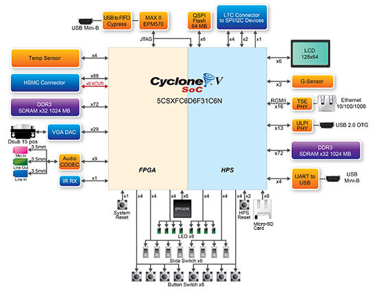
The SoCKit Development Kit presents a robust hardware design platform built around the Altera Cyclone V System-on-Chip (SoC) FPGA, which combines the latest Cortex-A9 embedded cores with industry-leading programmable logic for ultimate design flexibility. Users can now leverage the power of tremendous re-configurability paired with a high-performance, low-power processor system. Altera’s SoC integrates an ARM-based hard processor system (HPS) consisting of processor, peripherals and memory interfaces tied seamlessly with the FPGA fabric using a high-bandwidth interconnect backbone. The SoCKit development board includes hardware such as high-speed DDR3 memory, video and audio capabilities, Ethernet networking, and much more. In addition, an on-board HSMC connector with high-speed transceivers allows for an even greater array of hardware setups. By leveraging all of these capabilities, the SoCKit is the perfect solution for showcasing, evaluating, and prototyping the true potential of the Altera SoC.
FPGA Device
- Cyclone V SX SoC—5CSXFC6D6F31C6N
- 110K LEs, 41509 ALMs
- 5140 M10K memory blocks
- 6 FPGA PLLs and 3 HPS PLLs
- 2 Hard Memory Controllers
- 3.125G Transceivers
ARM®-based hard processor system (HPS)
- 925 MHz, A Dual-Core ARM Cortex™-A9 MPCore™ Processor
- 512 KB of shared L2 cache
- 64 KB of scratch RAM
- Multiport SDRAM controller with support for DDR2, DDR3, LPDDR1, and LPDDR2
- 8-channel direct memory access (DMA) controller
Configuration and Debug
- Quad Serial Configuration device – EPCQ256 for FPGA
- On-Board USB Blaster II (mini USB type B connector)
Memory Devices
- 1GB (2x256MBx16) DDR3 SDRAM on FPGA
- 1GB (2x256MBx16) DDR3 SDRAM on HPS
- 64MB QSPI Flash on HPS
- Micro-SD Card Socket on HPS
- EPCQ256 Flash on FPGA
Communication
- USB 2.0 OTG (ULPI interface with mini USB type AB connector)
- USB to UART (mini USB type B connector)
- 10/100/1000 Ethernet
Connectors
- One HSMC (8-channel Transceivers, Configurable I/O standards 1.5/1.8/2.5/3.3V)
- One LTC connector (One Serial Peripheral Interface (SPI) Master ,one I2C and one GPIO interface )
Display
- 24-bit VGA DAC
- 128x64 dots LCD Module with Backlight
Audio
- 24-bit CODEC, Line-in, line-out, and microphone-in jacks
Switches, Buttons and LEDs
- 8 User Keys (FPGA x4 ; HPS x 4)
- 8 User Switches (FPGA x4 ; HPS x 4)
- 8 User LEDs (FPGA x4 ; HPS x 4)
- 2 HPS Reset Buttons (HPS_RSET_n and HPS_WARM_RST_n)
Sensors
- G-Sensor on HPS
- Temperature Sensor on FPGA
Power
- 12V DC input
Block Diagram of the SoCKit Board
Related products


")


