- TRANSDUCERS
- TRANSDUCERS
- BASIC COMPONENTS DK
- BASIC COMPONENTS DK
- MARKETPLACE
- MARKETPLACE
- DEVELOPMENT BOARDS & KITS
- DEVELOPMENT BOARDS & KITS
- CABLE ASSEMBLIES
- CABLE ASSEMBLIES
- RF AND WIRELESS
- RF AND WIRELESS
- BOXES ENCLOSURES RACKS
- BOXES ENCLOSURES RACKS
- AUDIO PRODUCTS
- AUDIO PRODUCTS
- FANS-BLOWERS-THERMAL MANAGEMENT
- FANS-BLOWERS-THERMAL MANAGEMENT
- WIRELESS MODULES
- WIRELESS MODULES
- TERMINALS
- TERMINALS
- Cables/Wires
- Cables/Wires
- SINGLE BOARD COMPUTER
- SINGLE BOARD COMPUTER
- BREAKOUT BOARDS
- BREAKOUT BOARDS
- LED
- LED
- TEST AND MEASUREMENT
- TEST AND MEASUREMENT
- POTENTIONMETERS AND VARIABLE RESISTORS
- POTENTIONMETERS AND VARIABLE RESISTORS
- DEVELOPMENT BOARDS AND IC's
- DEVELOPMENT BOARDS AND IC's
- EMBEDDED COMPUTERS
- EMBEDDED COMPUTERS
- OPTOELECTRONICS
- OPTOELECTRONICS
- INDUSTRAL AUTOMATION AND CONTROL
- INDUSTRAL AUTOMATION AND CONTROL
- COMPUTER EQUIPMENT
- COMPUTER EQUIPMENT
- CONNECTORS & INTERCONNECTS
- CONNECTORS & INTERCONNECTS
- MAKER/DIY EDUCATIONAL
- MAKER/DIY EDUCATIONAL
- TOOLS
- TOOLS
- MOTORS/ACTUATORS/SOLEENOIDS/DRIVERS
- MOTORS/ACTUATORS/SOLEENOIDS/DRIVERS
- FPGA HARDWARE
- FPGA HARDWARE
- ROBOTICS & AUTOMATION
- ROBOTICS & AUTOMATION
Description
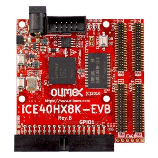
iCE40HX8K-EVB is low cost development board for iCE40 FPGA family from Lattice Semiconductor.
The interesting part about this family of FPGAs is that there is a completely free and open source development tool available.
Using this free tool you can compile Verilog designs and upload them to the FPGA. More inforomation on the link in Software section.
iCE40HX8K-EVB has 34 pin bus connector which allows the easy hardware expansion of the board with additional modules like: iCE40-ADC with 100Mhz ADC; iCE40-DAC with 100Mhz DAC; iCE40-IO with VGA, PS2 and IrDA transciever; MOD-DIO with logic analyzer level shifter with programmable 1.5-5.5V threshold. Up to 4 x ADC and 4 x DAC expansion modules can be connected on same bus (if you use iCE40-IO on the same bus then only up to 2 x ADC and 1 x DAC).
Features
- iCE40HX8K-CT256 FPGA 7680 Logic cells, 960 LABs, 128 K embedded RAM bits
- 512KB SRAM organized as 256Kx16bit 10ns
- 2MB Serial Flash
- 2 user status LEDs
- Programming successful status LED
- 2 user buttons
- Reset button
- Power jack for 5V DC external power supply
- PGM connector (all signals at PGM1 @ 3.3V DC)
- 34 pin connector bus
- 4 x 40 pin connectors for GPIOs
- 100 Mhz oscillator
- Power supply DCDC regulators
- Power supply status LED
- Dimentions: 65x67mm ~ (2.56x2.64)"
- Home
- iCE40HX8K-EVB
iCE40HX8K-EVB
SIZE GUIDE
- Shipping in 10-12 Working days
- http://cdn.storehippo.com/s/59c9e4669bd3e7c70c5f5e6c/ms.products/5db93cbd3aecaf3860d53a93/images/5db93cbd3aecaf3860d53a94/5db93c63a5e5252c9523a2a6/5db93c63a5e5252c9523a2a6.jpg
Description of product
Description
iCE40HX8K-EVB is low cost development board for iCE40 FPGA family from Lattice Semiconductor.
The interesting part about this family of FPGAs is that there is a completely free and open source development tool available.
Using this free tool you can compile Verilog designs and upload them to the FPGA. More inforomation on the link in Software section.
iCE40HX8K-EVB has 34 pin bus connector which allows the easy hardware expansion of the board with additional modules like: iCE40-ADC with 100Mhz ADC; iCE40-DAC with 100Mhz DAC; iCE40-IO with VGA, PS2 and IrDA transciever; MOD-DIO with logic analyzer level shifter with programmable 1.5-5.5V threshold. Up to 4 x ADC and 4 x DAC expansion modules can be connected on same bus (if you use iCE40-IO on the same bus then only up to 2 x ADC and 1 x DAC).
Features
- iCE40HX8K-CT256 FPGA 7680 Logic cells, 960 LABs, 128 K embedded RAM bits
- 512KB SRAM organized as 256Kx16bit 10ns
- 2MB Serial Flash
- 2 user status LEDs
- Programming successful status LED
- 2 user buttons
- Reset button
- Power jack for 5V DC external power supply
- PGM connector (all signals at PGM1 @ 3.3V DC)
- 34 pin connector bus
- 4 x 40 pin connectors for GPIOs
- 100 Mhz oscillator
- Power supply DCDC regulators
- Power supply status LED
- Dimentions: 65x67mm ~ (2.56x2.64)"
NEWSLETTER
Subscribe to get Email Updates!
Thanks for subscribe.
Your response has been recorded.
INFORMATION
ACCOUNT
ADDRESS
Tenet Technetronics# 2514/U, 7th 'A' Main Road, Opp. to BBMP Swimming Pool, Hampinagar, Vijayanagar 2nd Stage.
Bangalore
Karnataka - 560104
IN
Tenet Technetronics focuses on “Simplifying Technology for Life” and has been striving to deliver the same from the day of its inception since 2007. Founded by young set of graduates with guidance from ardent professionals and academicians the company focuses on delivering high quality products to its customers at the right cost considering the support and lifelong engagement with customers. “We don’t believe in a sell and forget model “and concentrate and building relationships with customers that accelerates, enhances as well as provides excellence in their next exciting project.


