- TRANSDUCERS
- TRANSDUCERS
- BASIC COMPONENTS DK
- BASIC COMPONENTS DK
- MARKETPLACE
- MARKETPLACE
- DEVELOPMENT BOARDS & KITS
- DEVELOPMENT BOARDS & KITS
- CABLE ASSEMBLIES
- CABLE ASSEMBLIES
- RF AND WIRELESS
- RF AND WIRELESS
- BOXES ENCLOSURES RACKS
- BOXES ENCLOSURES RACKS
- AUDIO PRODUCTS
- AUDIO PRODUCTS
- FANS-BLOWERS-THERMAL MANAGEMENT
- FANS-BLOWERS-THERMAL MANAGEMENT
- WIRELESS MODULES
- WIRELESS MODULES
- TERMINALS
- TERMINALS
- Cables/Wires
- Cables/Wires
- SINGLE BOARD COMPUTER
- SINGLE BOARD COMPUTER
- BREAKOUT BOARDS
- BREAKOUT BOARDS
- LED
- LED
- TEST AND MEASUREMENT
- TEST AND MEASUREMENT
- POTENTIONMETERS AND VARIABLE RESISTORS
- POTENTIONMETERS AND VARIABLE RESISTORS
- DEVELOPMENT BOARDS AND IC's
- DEVELOPMENT BOARDS AND IC's
- EMBEDDED COMPUTERS
- EMBEDDED COMPUTERS
- OPTOELECTRONICS
- OPTOELECTRONICS
- INDUSTRAL AUTOMATION AND CONTROL
- INDUSTRAL AUTOMATION AND CONTROL
- COMPUTER EQUIPMENT
- COMPUTER EQUIPMENT
- CONNECTORS & INTERCONNECTS
- CONNECTORS & INTERCONNECTS
- MAKER/DIY EDUCATIONAL
- MAKER/DIY EDUCATIONAL
- TOOLS
- TOOLS
- MOTORS/ACTUATORS/SOLEENOIDS/DRIVERS
- MOTORS/ACTUATORS/SOLEENOIDS/DRIVERS
- FPGA HARDWARE
- FPGA HARDWARE
- ROBOTICS & AUTOMATION
- ROBOTICS & AUTOMATION
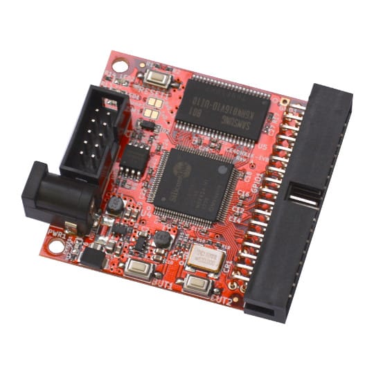
iProgrammable Logic IC Development Tools ICE40HX1K FPGA Development Board
| Product Attribute | Attribute Value | |
|---|---|---|
| Olimex Ltd. | ||
| Product Category: | Programmable Logic IC Development Tools | |
| RoHS: | ||
| Evaluation Boards | ||
| FPGA | ||
| iCE40HX1K | ||
| Brand: | Olimex Ltd. | |
| Dimensions: | 50 mm x 50 mm | |
| Interface Type: | Serial | |
| Operating Supply Voltage: | 5 V | |
| Product Type: | Programmable Logic IC Development Tools | |
| Subcategory: | Development Tools | |
- Home
- iCE40HX1K-EVB
iCE40HX1K-EVB
SIZE GUIDE
- Shipping in 10-12 Working days
Description of product
iProgrammable Logic IC Development Tools ICE40HX1K FPGA Development Board
| Product Attribute | Attribute Value | |
|---|---|---|
| Olimex Ltd. | ||
| Product Category: | Programmable Logic IC Development Tools | |
| RoHS: | ||
| Evaluation Boards | ||
| FPGA | ||
| iCE40HX1K | ||
| Brand: | Olimex Ltd. | |
| Dimensions: | 50 mm x 50 mm | |
| Interface Type: | Serial | |
| Operating Supply Voltage: | 5 V | |
| Product Type: | Programmable Logic IC Development Tools | |
| Subcategory: | Development Tools | |
NEWSLETTER
Subscribe to get Email Updates!
Thanks for subscribe.
Your response has been recorded.
INFORMATION
ACCOUNT
ADDRESS
Tenet Technetronics# 2514/U, 7th 'A' Main Road, Opp. to BBMP Swimming Pool, Hampinagar, Vijayanagar 2nd Stage.
Bangalore
Karnataka - 560104
IN
Tenet Technetronics focuses on “Simplifying Technology for Life” and has been striving to deliver the same from the day of its inception since 2007. Founded by young set of graduates with guidance from ardent professionals and academicians the company focuses on delivering high quality products to its customers at the right cost considering the support and lifelong engagement with customers. “We don’t believe in a sell and forget model “and concentrate and building relationships with customers that accelerates, enhances as well as provides excellence in their next exciting project.


