- TRANSDUCERS
- TRANSDUCERS
- BASIC COMPONENTS DK
- BASIC COMPONENTS DK
- MARKETPLACE
- MARKETPLACE
- DEVELOPMENT BOARDS & KITS
- DEVELOPMENT BOARDS & KITS
- CABLE ASSEMBLIES
- CABLE ASSEMBLIES
- RF AND WIRELESS
- RF AND WIRELESS
- BOXES ENCLOSURES RACKS
- BOXES ENCLOSURES RACKS
- AUDIO PRODUCTS
- AUDIO PRODUCTS
- FANS-BLOWERS-THERMAL MANAGEMENT
- FANS-BLOWERS-THERMAL MANAGEMENT
- WIRELESS MODULES
- WIRELESS MODULES
- TERMINALS
- TERMINALS
- Cables/Wires
- Cables/Wires
- SINGLE BOARD COMPUTER
- SINGLE BOARD COMPUTER
- BREAKOUT BOARDS
- BREAKOUT BOARDS
- LED
- LED
- TEST AND MEASUREMENT
- TEST AND MEASUREMENT
- POTENTIONMETERS AND VARIABLE RESISTORS
- POTENTIONMETERS AND VARIABLE RESISTORS
- DEVELOPMENT BOARDS AND IC's
- DEVELOPMENT BOARDS AND IC's
- EMBEDDED COMPUTERS
- EMBEDDED COMPUTERS
- OPTOELECTRONICS
- OPTOELECTRONICS
- INDUSTRAL AUTOMATION AND CONTROL
- INDUSTRAL AUTOMATION AND CONTROL
- COMPUTER EQUIPMENT
- COMPUTER EQUIPMENT
- CONNECTORS & INTERCONNECTS
- CONNECTORS & INTERCONNECTS
- MAKER/DIY EDUCATIONAL
- MAKER/DIY EDUCATIONAL
- TOOLS
- TOOLS
- MOTORS/ACTUATORS/SOLEENOIDS/DRIVERS
- MOTORS/ACTUATORS/SOLEENOIDS/DRIVERS
- FPGA HARDWARE
- FPGA HARDWARE
- ROBOTICS & AUTOMATION
- ROBOTICS & AUTOMATION
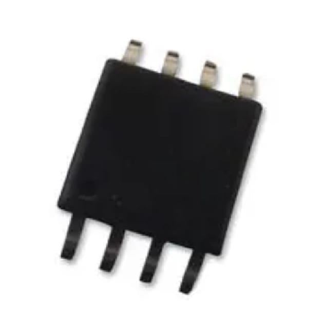
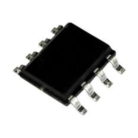
The AT45DB641E is a 1.7V minimum, serial-interface sequential access Flash memory ideally suited for a wide variety of digital voice, image, program code, and data storage applications. The AT45DB641E also supports the RapidS serial interface for applications requiring very high speed operation. Its 69,206,016 bits of memory are organized as 32,768 pages of 256 bytes or 264 bytes each. In addition to the main memory, the AT45DB641E also contains two SRAM
buffers of 256/264 bytes each. Interleaving between both buffers can dramatically increase a system’s ability to write a continuous data stream. In addition, the SRAM buffers can be used as additional system scratch pad memory, and E2 PROM emulation (bit or byte alterability) can be easily handled with a self-contained three step read-modify-write operation.
Unlike conventional Flash memories that are accessed randomly with multiple address lines and a parallel interface, the DataFlash® uses a serial interface to sequentially access its data. The simple sequential access dramatically reduces active pin count, facilitates simplified hardware layout, increases system reliability, minimizes switching noise, and
reduces package size. The device is optimized for use in many commercial and industrial applications where high-density, low-pin count, low-voltage, and low-power are essential.
To allow for simple in-system re-programmability, the AT45DB641E does not require high input voltages for programming. The device operates from a single 1.7V to 3.6V power supply for the erase and program and read operations. The AT45DB641E is enabled through the Chip Select pin (CS) and accessed via a 3-wire interface consisting of the Serial Input (SI), Serial Output (SO), and the Serial Clock (SCK). All programming and erase cycles are self-timed.
Features:
- Single 1.7V – 3.6V supply
- Program and Erase Suspend/Resume
- Hardware and software controlled reset options
- JEDEC Standard Manufacturer and Device ID Read
- Endurance: 100,000 program/erase cycles per page minimum
- Data retention: 20 years
- Complies with full industrial temperature range
Package Includes:
1 x AT45DB641E-SHN-B-RENESAS-Flash Memory, DataFlash, Serial NOR, 64Mbit, 32K Pages x 264Byte, SPI, WSOIC-8
- Home
- MARKETPLACE
- AT45DB641E-SHN-B-RENESAS-Flash Memory, DataFlash, Serial NOR, 64Mbit, 32K Pages x 264Byte, SPI, WSOIC-8
AT45DB641E-SHN-B-RENESAS-Flash Memory, DataFlash, Serial NOR, 64Mbit, 32K Pages x 264Byte, SPI, WSOIC-8
SIZE GUIDE
- Shipping in 10-12 Working Days
Description of product
The AT45DB641E is a 1.7V minimum, serial-interface sequential access Flash memory ideally suited for a wide variety of digital voice, image, program code, and data storage applications. The AT45DB641E also supports the RapidS serial interface for applications requiring very high speed operation. Its 69,206,016 bits of memory are organized as 32,768 pages of 256 bytes or 264 bytes each. In addition to the main memory, the AT45DB641E also contains two SRAM
buffers of 256/264 bytes each. Interleaving between both buffers can dramatically increase a system’s ability to write a continuous data stream. In addition, the SRAM buffers can be used as additional system scratch pad memory, and E2 PROM emulation (bit or byte alterability) can be easily handled with a self-contained three step read-modify-write operation.
Unlike conventional Flash memories that are accessed randomly with multiple address lines and a parallel interface, the DataFlash® uses a serial interface to sequentially access its data. The simple sequential access dramatically reduces active pin count, facilitates simplified hardware layout, increases system reliability, minimizes switching noise, and
reduces package size. The device is optimized for use in many commercial and industrial applications where high-density, low-pin count, low-voltage, and low-power are essential.
To allow for simple in-system re-programmability, the AT45DB641E does not require high input voltages for programming. The device operates from a single 1.7V to 3.6V power supply for the erase and program and read operations. The AT45DB641E is enabled through the Chip Select pin (CS) and accessed via a 3-wire interface consisting of the Serial Input (SI), Serial Output (SO), and the Serial Clock (SCK). All programming and erase cycles are self-timed.
Features:
- Single 1.7V – 3.6V supply
- Program and Erase Suspend/Resume
- Hardware and software controlled reset options
- JEDEC Standard Manufacturer and Device ID Read
- Endurance: 100,000 program/erase cycles per page minimum
- Data retention: 20 years
- Complies with full industrial temperature range
Package Includes:
1 x AT45DB641E-SHN-B-RENESAS-Flash Memory, DataFlash, Serial NOR, 64Mbit, 32K Pages x 264Byte, SPI, WSOIC-8
Related products
NEWSLETTER
Subscribe to get Email Updates!
Thanks for subscribe.
Your response has been recorded.
INFORMATION
ACCOUNT
ADDRESS
Tenet Technetronics# 2514/U, 7th 'A' Main Road, Opp. to BBMP Swimming Pool, Hampinagar, Vijayanagar 2nd Stage.
Bangalore
Karnataka - 560104
IN
Tenet Technetronics focuses on “Simplifying Technology for Life” and has been striving to deliver the same from the day of its inception since 2007. Founded by young set of graduates with guidance from ardent professionals and academicians the company focuses on delivering high quality products to its customers at the right cost considering the support and lifelong engagement with customers. “We don’t believe in a sell and forget model “and concentrate and building relationships with customers that accelerates, enhances as well as provides excellence in their next exciting project.


