


Altera Cyclone III FPGA Development Kit
- Shipping in 10-12 Working days
- http://cdn.storehippo.com/s/59c9e4669bd3e7c70c5f5e6c/ms.products/5b939d096d77b0b20491b72a/images/5b939d096d77b0b20491b72b/5b939cd1b7167eb27e67ebe7/5b939cd1b7167eb27e67ebe7.jpg
Description of product
Description
Altera's Cyclone III FPGA Development Kit combines the largest density low-cost, low-power FPGA available with a robust set of memories and user interfaces. The kit dramatically reduces the design and verification portion of your project, whether it’s for automotive, consumer, wireless communications, video processing or another high-volume, cost-sensitive application.
The low-cost Cyclone III FPGA family—the industry’s first family of low-cost, 60-nm devices—offers an unprecedented combination of low power, high functionality, and low cost. Cyclone III devices are ideal to complement or replace ASSPs or ASICs.
If you are an experienced FPGA designer checking out the Cyclone III architecture, you'll love building systems leveraging the 50 percent (on average) faster performance Cyclone III FPGAs offer over the competition.
Cyclone III development board
- Cyclone III EP3C120F780 FPGA
- Embedded USB-Blaster™ circuitry (includes an Altera MAX® II CPLD) allowing download of FPGA configuration files via the flash device or the host computer
Memory
- 256 megabytes (MB) of dual-channel DDR2 SDRAM with error correction code (ECC)
- 8 MB of synchronous SRAM
- 64 MB of flash memory
Communication ports
- 10/100/1000 Ethernet
- USB 2.0
Power and analog devices from Linear Technology
- Switching power supply LTM4601
- Switching and step-down regulators LT1931 , LT3481 , and LTC3418
- Analog-to-digital converter LTC2402
- LDO regulators LT1963 and LT1761
Clocking
- 50-MHz and 125-MHz on-board oscillators
- SMA inputs/outputs
- I/Os for the two HSMC connectors
- Various buttons, switches, and indicators
Display
- 128 x 64 graphics LCD
- 2-line x 16-character LCD
Connectors
- Two HSMCs
- USB type B
Debug tools
- Three HSMC debug cards (two loop-back and a debug header)
Cables and power/analog
- 14-V to 20-V DC input
- On-board power measurement circuitry
- 19.8 W per HSMC interface
- Power cord with plug adapters (U.S., UK, and EU)
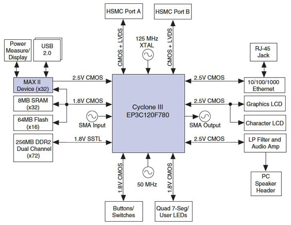
Altera Cyclone III Development Board Block Diagram
Related products


")


