
-
TERMINALS
- TERMINALS
-
WIRELESS MODULES
- WIRELESS MODULES
-
DEVELOPMENT BOARDS & KITS
- DEVELOPMENT BOARDS & KITS
-
RF and Wireless
- RF and Wireless
-
SINGLE BOARD COMPUTER
- SINGLE BOARD COMPUTER
-
BREAKOUT BOARDS
- BREAKOUT BOARDS
-
LED
- LED
-
LCD & DISPLAYS
- LCD & DISPLAYS
-
TEST AND MEASUREMENT
- TEST AND MEASUREMENT
-
DEVELOPMENT BOARDS AND IC's
- DEVELOPMENT BOARDS AND IC's
-
CABLES/WIRES/FANS
- CABLES/WIRES/FANS
-
EMBEDDED COMPUTERS
- EMBEDDED COMPUTERS
-
INDUSTRAL AUTOMATION AND CONTROL
- INDUSTRAL AUTOMATION AND CONTROL
-
COMPUTER EQUIPMENT
- COMPUTER EQUIPMENT
-
CONNECTORS & INTERCONNECTS
- CONNECTORS & INTERCONNECTS
-
MOTORS/DRIVERS/ACTUATORS/MODULES
- MOTORS/DRIVERS/ACTUATORS/MODULES
-
MAKER/DIY EDUCATIONAL
- MAKER/DIY EDUCATIONAL
-
BASIC COMPONENTS
- BASIC COMPONENTS
-
TOOLS & ACCESSORIES
- TOOLS & ACCESSORIES
-
FPGA HARDWARE
- FPGA HARDWARE
-
ARTILA
- ARTILA
-
POWER SUPPLIES
- POWER SUPPLIES
-
ROBOTICS & AUTOMATION
- ROBOTICS & AUTOMATION
-
TRANSDUCERS
- TRANSDUCERS
-
MEMORY CARDS & MODULES
- MEMORY CARDS & MODULES
-
SOFTWARE
- SOFTWARE

Description
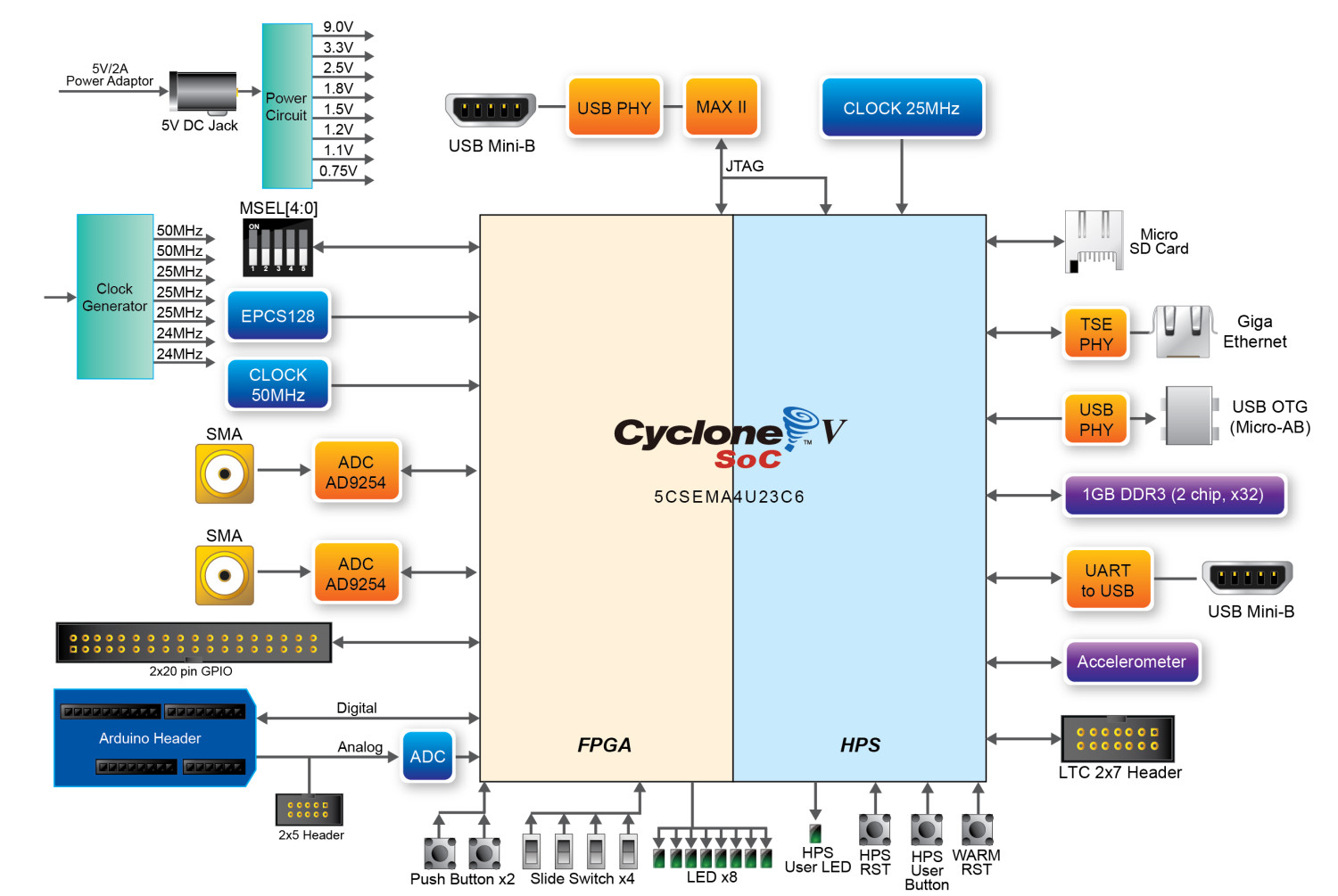
The ADC-SoC is a SoC FPGA motherboard with dual-channel high-speed ADC. The main card is based on the Terasic DE0-Nano-SoC board with a built-in high-speed ADC circuit on the DCC (AD / DA Data Conversion Card) on top of the main card. This feature makes the board an ideal platform for systems that require high-speed ADC applications.
The built-in ADC circuit uses SMA as the input interface. The circuit provides two channels, each with 14-bit resolution and a sample rate of up to 150 MSPS (Megasamples per Second).
FPGA Device
- Altera Cyclone® V SE 5CSEMA4U23C6N device
- Serial configuration device – EPCS128
- USB-Blaster II onboard for programming; JTAG Mode
- 2 push-buttons
- 4 slide switches
- 8 green user LEDs
- Three 50MHz clock sources from the clock generator
- One 40-pin expansion header
- One Arduino expansion header (Uno R3 compatibility), can connect with Arduino shields
- One 10-pin Analog input expansion header (shared with Arduino Analog input)
- A/D converter, 4-pin SPI interface with FPGA
- Two 14-bit AD Converters with 150 MSPS (Mega-Samples per Second)
HPS (Hard Processor System)
- 925MHz Dual-core ARM Cortex-A9 processor
- 1GB DDR3 SDRAM (32-bit data bus)
- 1 Gigabit Ethernet PHY with RJ45 connector
- USB OTG Port, USB Micro-AB connector
- Micro SD card socket
- Accelerometer (I2C interface + interrupt)
- UART to USB, USB Mini-B connector
- Warm reset button and cold reset button
- One user button and one user LED
- LTC 2x7 expansion header
- On-Board RTC (Real-Time Clock)
HIgh Speed AD (Analog-to-Digital) Conversion
- Two channels
- 14-bit resolution
- Up to 150MSPS (Mega-Samples per Second)
Block Diagram of the ADC-SOC Board
- Home
- FPGA HARDWARE
- INTEL FPGA
- ADC-SoC

ADC-SoC
SIZE GUIDE
- Shipping in 10-12 Working days
- http://cdn.storehippo.com/s/59c9e4669bd3e7c70c5f5e6c/ms.products/5b924c6328374760bf6c89ed/images/5b924c6328374760bf6c89ee/5b924c2dd9b3437fe7e09a30/5b924c2dd9b3437fe7e09a30.jpg
Description of product
Description
The ADC-SoC is a SoC FPGA motherboard with dual-channel high-speed ADC. The main card is based on the Terasic DE0-Nano-SoC board with a built-in high-speed ADC circuit on the DCC (AD / DA Data Conversion Card) on top of the main card. This feature makes the board an ideal platform for systems that require high-speed ADC applications.
The built-in ADC circuit uses SMA as the input interface. The circuit provides two channels, each with 14-bit resolution and a sample rate of up to 150 MSPS (Megasamples per Second).
FPGA Device
- Altera Cyclone® V SE 5CSEMA4U23C6N device
- Serial configuration device – EPCS128
- USB-Blaster II onboard for programming; JTAG Mode
- 2 push-buttons
- 4 slide switches
- 8 green user LEDs
- Three 50MHz clock sources from the clock generator
- One 40-pin expansion header
- One Arduino expansion header (Uno R3 compatibility), can connect with Arduino shields
- One 10-pin Analog input expansion header (shared with Arduino Analog input)
- A/D converter, 4-pin SPI interface with FPGA
- Two 14-bit AD Converters with 150 MSPS (Mega-Samples per Second)
HPS (Hard Processor System)
- 925MHz Dual-core ARM Cortex-A9 processor
- 1GB DDR3 SDRAM (32-bit data bus)
- 1 Gigabit Ethernet PHY with RJ45 connector
- USB OTG Port, USB Micro-AB connector
- Micro SD card socket
- Accelerometer (I2C interface + interrupt)
- UART to USB, USB Mini-B connector
- Warm reset button and cold reset button
- One user button and one user LED
- LTC 2x7 expansion header
- On-Board RTC (Real-Time Clock)
HIgh Speed AD (Analog-to-Digital) Conversion
- Two channels
- 14-bit resolution
- Up to 150MSPS (Mega-Samples per Second)
Block Diagram of the ADC-SOC Board
Related products


")


NEWSLETTER
Subscribe to get Email Updates!
Thanks for subscribe.
Your response has been recorded.
INFORMATION
ACCOUNT
ADDRESS
Tenet Technetronics# 2514/U, 7th 'A' Main Road, Opp. to BBMP Swimming Pool, Hampinagar, Vijayanagar 2nd Stage.
Bangalore
Karnataka - 560104
IN
Tenet Technetronics focuses on “Simplifying Technology for Life” and has been striving to deliver the same from the day of its inception since 2007. Founded by young set of graduates with guidance from ardent professionals and academicians the company focuses on delivering high quality products to its customers at the right cost considering the support and lifelong engagement with customers. “We don’t believe in a sell and forget model “and concentrate and building relationships with customers that accelerates, enhances as well as provides excellence in their next exciting project.